How to make better electrical contacts with graphene nanoribbons
By Nicola Nosengo, NCCR MARVEL
Graphene nanoribbons (GNRs) are one-dimensional materials that have great potential as components in nano-electronic devices. Because they are made of graphene, they have excellent electron mobility (although reduced by the opening of the gap and confinement), and because they are ribbons – which is, strips of graphene with widths in the order of only a few nm - they have a bandgap, which can be finely tuned by adjusting their width and edge topology. This makes them ideal for components such as field-effect transistors, where they could one day replace silicon, provided they can guarantee the same level of performance. As of today, the big challenge is making contacts between GNRs and electrodes. The fabrication techniques used so far consisted in placing the ribbons above (or below) metallic electrodes and tend to result in a prominent influence of the contact resistance, also potentially introducing impurities affecting the performance of the GNR device.
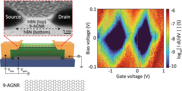
To overcome these challenges, a group of Switzerland-based scientists has used a mix of experimental and theoretical models to develop a different technique: incapsulating nanoribbons in hexagonal boron-nitride (h-BN), and using a new kind of contact where the ribbon and the electrode are placed side by side, rather than one on top of the other. The result is a more predictable electric behavior, potentially suitable for a transistor and quantum technologies. The authors of the study, published in ACS Nano, include MARVEL members Daniele Passerone, from the Swiss Federal Laboratories for Materials Science and Technology, in Dübendorf, and Mathieu Luisier, from ETH Zurich.
The study was based on one of the most studied GNR configurations: a ribbon that is 9 atoms wide, with edges of the “armchair” type. This is one of the two high-symmetry configurations for graphene nanoribbons, the other being the “zig-zag” type. “It is the most studied type of ribbon”, says Passerone. “It is robust, it survives many conditions, it has a suitable bandgap for switching at room temperature, and it can grow very long. In this study the GNR average length was in the order of 45 nanometers, now we have reached up to 70 nanometers”.
ACS Nano, 2023
Encapsulating the ribbon in hexagonal boron nitride allows to protect both the ribbon and the electrode from electrostatic effects and minimize damage to the junction. “But it is very challenging to manufacture because you have to exfoliate hexagonal boron nitride and place a layer of it below and above the ribbon and create electrode gaps in the same order of the GNR length,” explains Passerone “It had already been done for two-dimensional materials in micrometer scale but very rarely for one-dimensional ones”.
The most important innovation in the study, though, is the design of the contacts. “In most other studies the ribbon was placed on the top of the contact electrode, which causes interaction with van der Waals forces (or in case of metal electrode, weak chemical interactions) and a number of other problems,” says Passerone. The edge contact instead creates a more stable contact interface between ribbon and electrode. As for materials, the electrode used in the study is made out of a chromium-palladium alloy.
“The original electrodes in the 2017 device by scientists at Berkeley was based on palladium, and different other electrodes were tried in the literature, but this alloy is more processable and chromium improves the contact because of the chemistry at the local level”.
Once the transistor was successfully fabricated, the scientists computed its bandgap and electronic properties using density functional theory (DFT) and dedicated methods for computing electronic transport in the complete structure including the metal contacts. The computational strategy starts with the determination of a stable interfacial structure between the ribbon and the metal surface (done with DFT); the resulting structure and the corresponding DFT electronic structure is used as an input for the non-equilibrium Green’s function formalism to calculate the transmission function and the current. The extension to low-temperature properties requires more advanced methods that keep into account electronic correlation at a higher level, presently under development in the Empa research groups. As a main result, the scientists also characterized the transistor in experiments.
They concluded that its electronic properties vary with temperature: up to 9 K, the device behaves like a quantum dot, thus resembling a single atom. Temperature-activated hopping of charges through the ribbon appears and starts to dominate above 100 K, while at room temperature, the transistor behaves like a semiconductor.
In addition to the possible use in nanotransistors, this behaviour could be exploited for different applications. “If we could bring the quantum dot behavior closer to room temperature, this could have applications in quantum computing,” says Passerone. “One could have a ribbon that behaves like a quantum dot, then have another one a few nanometers apart, and have interactions between quantum dots. This way, you can create regions of quantum dots and play with distances and electric fields and create a sort of sandbox of quantum dot control and interaction that is at the basis for quantum computing”.
There is still a long way to go before this experimental contact can scale-up to a device that can be used at the industrial level. “But having a proof of concept is very important, as is the fact that we were able to measure different kinds of transport,” says Passerone. “In the future, we could try other configurations using different ribbons with different bandgaps, different ranges of temperature. The quantum behavior depends on the width of the ribbon, not the length, and in principle, a very long ribbon would still give you the quantum behavior while making it easier to integrate it into a device”. Even more fascinating is the perspective of including in GNRs spin chains or quantum phases that are topologically protected - all structures that have been already realized in the laboratory of Roman Fasel and Gabriela Borin Barin at Empa. This highlights the importance of the encapsulation, that is crucial to extend device integration to GNRs that are sensitive to ambient conditions such as spin chains and topological GNRs.
Reference
W. Huang, O. Braun, D. I. Indolese, G. Borin Barin, G. Gandus, M. Stiefel, A. Olziersky, K. Müllen, M. Luisier, D. Passerone, P. Ruffieux, C. Schönenberger, K. Watanabe, T. Taniguchi, R. Fasel, J. Zhang, M. Calame, and M. L. Perrin, "Edge Contacts to Atomically Precise Graphene Nanoribbons", ACS Nano 2023, https://doi.org/10.1021/acsnano.3c00782
Low-volume newsletters, targeted to the scientific and industrial communities.
Subscribe to our newsletter