MARVEL team shows how properties of amorphous aluminum oxide can be tuned by electrochemical anodizing
by Carey Sargent, EPFL, NCCR MARVEL

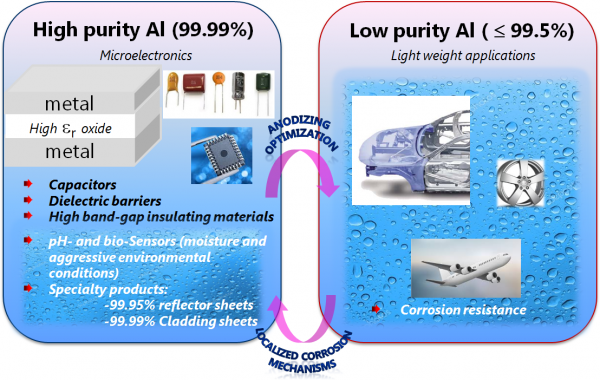
Figure 1. Application domain for thin aluminum oxides
“Aluminum oxide is an interesting material with properties that are very relevant for industrial applications ranging from microelectronics to lightweight transportation,” —Claudia Cancellieri, Empa
Scientists including Empa’s Claudia Cancellieri and Patrik Schmutz chose to study defect distribution in “thin” amorphous aluminum oxides because there is still an enormous knowledge gap concerning properties including stability in harsh environments, electronic and surface reactivity of these non-crystalline structures. From the perspective of industrial applications, it is often impossible to obtain thin defect-free and perfectly crystallized aluminum oxides. Nonetheless, since there is little reliable information on the real surface oxide, component design is based on the properties of perfect oxides and this often leads to reliability issues and the incorrect estimation of component lifetimes.
“Aluminum oxide is an interesting material with properties that are very relevant for industrial applications ranging from microelectronics to lightweight transportation,” Cancellieri said (See Figure 1). “And while you can study ideal crystalline systems, they don’t represent reality. Deposited or natively grown thin oxides present on the surface of real industrial components are defective, far from perfect, and that’s what we are studying in our MARVEL project.”
In terms of electrochemical anodic oxide growth, or the anodizing method, much past research has been done on the growth mechanisms of porous alumina, which is used in applications such as templates for the synthesis of nanowires and nanotubes, but mainly as a corrosion protection barrier. In the MARVEL study, thinner barrier-type anodic aluminum oxides, which could be used in dielectric capacitors or protecting vacuum-deposited materials and small structures, have been studied as a model amorphous oxide.
Barrier anodizing is a process used to increase the thickness of the natural oxide layer on the surface of metals and involves passing a direct current through an electrolytic solution. The electrochemical growth method has several advantages, including a very precise applied voltage-dependent oxide thickness control (from 20 up to 500 nm in the MARVEL study), a better lateral homogeneity compared to most oxide deposition techniques for large surfaces and room-temperature processing, which is then interesting for small heat-sensitive structures.
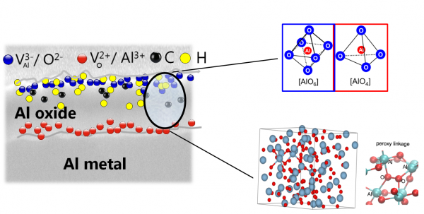
The first round of studies carried out at Empa involved investigating the effect of different anodizing potentials of up to 350 volts on the structural (defect level, density, morphology) and dielectric properties of the aluminum oxides. Using various techniques including x-ray diffraction, scanning electron microscopy and AFM-based Scanning Kelvin Probe Force Microscopy, the scientists found that generating the oxide layers at different voltages resulted in amorphous oxides with changing surface morphology and structural defects, but also in changes in density and dielectric constant. (See Figure 2, which displays the typical barrier oxide layer obtained through anodizing)

Figure 2. Schematic defect representation of anodically grown amorphous oxides.
"Our contribution to this was really providing support from the theoretical side in both the interpretation of the results and finding a possible explanation for them.” —Alfredo Pasquarello, EPFL
The oxides are laterally very homogeneous, with no defects at the nm-scale that would allow current flow. On the other side, different types and level of vacancies are present that can be filled by small impurities such as hydrogen and carbons. The presence of different types of Al coordination in the oxides could be identified by EXAFS measurements. As this local ordering forms the building blocks of amorphous Al-oxide, it became clear that defect level and cluster organization would play a significant role in density variation and resulting electronic properties.
The next step was to examine these experimental results in more detail. That’s when the Empa team sought assistance from theoreticians because interpreting the structure-property relationship was not straightforward. “You don’t find so many theoretical groups interested to work on amorphous oxides,” Empa’s Schmutz said. “From a modelling point of view, as soon as you have a lack of structure and order, it makes all the calculations extremely complicated and the approach different.”
They nonetheless found an experienced partner in a group led by EPFL’s Alfredo Pasquarello. Using the experimental observations as a starting point, Pasquarello and his group set to work on developing a theory that could explain the data. The experimental results had indicated that a main physical property that distinguished the grown oxides one from the other was the dielectric constant. The researchers considered what could account for this and, based on the observed results, hypothesized that there may be a correlation between the density of the amorphous oxide and its dielectric properties.
“It was natural to think that density might lead to such an effect in this material and so in the end that’s what we explored from a theoretical point of view,” Pasquarello said. “We got some results that indicated that the type of trends observed experimentally could indeed be explained by this kind of amorphous oxide (Fig.2) density dependence. Our contribution to this was really providing support from the theoretical side in both the interpretation of the results and finding a possible explanation for them.”
Results from the MARVEL project showed then that changing the anodizing potential but also underlying substrate purity affects the defect level, density and dielectric constant of the resulting oxide— specifically, that density can be raised through higher anodizing voltages—indicating that the process is a precise technique for producing barrier-type oxides with tunable properties. This is particularly interesting for industry because the resulting knowledge could allow for the growth of dense amorphous structure with few defects, producing a material with very good barrier properties that could be used in applications such as gate insulator materials.
Ongoing research shows that the grown amorphous oxides also have very different semiconductor properties depending on the atomic scale defects density and types. A second phase of the project is therefore investigating their semiconductor properties with a focus on the influence of the underlying substrates on the growth mechanisms and oxide defect level.
The studies have so far shown that, depending on the oxide “structure” and defect density, the electronic properties “are far, from the alumina predicted insulating behavior mentioned in textbook,” Schmutz said. The findings on these properties, which also influence surface reactivity and corrosion resistance, are relevant in a fairly wide field.
Low-volume newsletters, targeted to the scientific and industrial communities.
Subscribe to our newsletter