Strain modifies the valley structure of 2D materials, leads to remarkable improvements in conductivity
by Carey Sargent, NCCR MARVEL, EPFL
Two-dimensional (2D) materials—substances just a few nanometers thick—have shown numerous novel properties, making them attractive candidates for use in potential applications such as in optoelectronic and semiconducting devices. Their thinness makes them particularly suitable for applications in conventional and flexible electronics.
The performance of such devices largely depends on high carrier mobility, a measure of how quickly electrons and holes can move through a material when pulled by an electric field. While graphene excels in this area—it is currently the best electrical conductor we know of—it also features a gapless band structure: electrons move freely and there is no “off“ state associated with zero current flow. This lack of an “on-off switch” means the materials cannot be used as such in logical devices. Other well-known 2D materials such as transition metal dichalcogenides (TMDs) have the necessary band gaps but have relatively poor carrier mobilities. There is a pressing need for 2D semiconductors that combine both attributes.
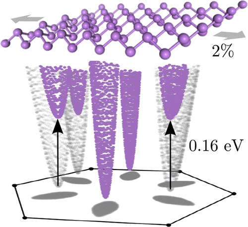
In arsenene a 2% strain stops scattering into four of the six valleys and leads to a 600% increase in mobility.
Designing or discovering such materials requires that the scattering processes that degrade electrical transport be minimized. Since external scattering sources such as impurities can be controlled through the systematic improvement of sample quality, design strategies should rather focus on maximizing intrinsic performance.
A good starting point is a focus on electron-phonon interactions: phonons play a dominant role in limiting the intrinsic mobility of a material, especially at room temperature. The presence of multiple valleys within an energy range compatible with phonon frequencies leads to significant phonon-assisted intervalley scattering and this has detrimental effects on mobility. While it is not the only scattering mechanism present, intervalley electron-phonon coupling is large in well-known 2D semiconductors. Indeed, there is a simple correlation between the number of valleys and the intrinsic mobility. It may therefore be possible to enhance electronic performance by engineering the valley structure such that intervalley electron-phonon scattering is suppressed.
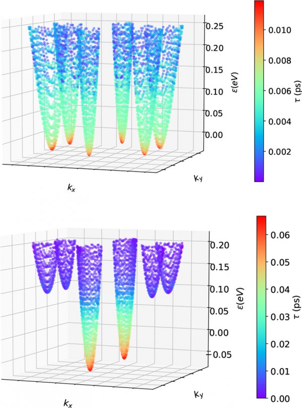
Scattering times for equilibrium and strained arsenene.
One way of doing this may be to exploit the extreme sensitivity of 2D materials to external manipulations. Such materials can be easily stretched up, for example, and it has been shown that strain plays an important role in determining their electronic and optical properties. For instance, strain fields open a gap in graphene on boron nitride, change the gap from direct to indirect in antimonene or TMDs, allow the manipulation of spin and valley transport, and reduce the band gap of TMDs.
In the paper “Valley-engineering mobilities in 2D materials" published in Nano Letters, NCCR MARVEL researchers suggest that strain is a viable way to engineer the valley structure of 2D materials. As an example, they investigate arsenene—a monolayer of arsenic atoms forming a buckled hexagonal honeycomb structure—as a prototypical example because of its six multivalley conduction bands. They show that a relatively small strain is enough to push four of these arsenene valleys high enough in energy to effectively suppress all corresponding intervalley scattering processes. This in turn greatly enhances electron mobility—in this case, the enhancement factor was on the order of 600%.
The researchers expect similar results for group-V buckled mono-layers or other multivalley 2D materials. They show, for example, that the same features are also present in antimonene and blue phosphorene. They reckon that about a third of the 2D materials in their database—available on the Materials Cloud platform here—could show the same effect.
Reference: Valley-engineering mobilities in 2D materials
Thibault Sohier*† , Marco Gibertini‡, Davide Campi†, Giovanni Pizzi†, and Nicola Marzari†
† Theory and Simulation of Materials (THEOS), and National Centre for Computational Design and Discovery of Novel Materials (MARVEL), École Polytechnique Fédérale de Lausanne, CH-1015 Lausanne, Switzerland
‡ Department of Quantum Matter Physics, University of Geneva, CH-1211 Geneva, Switzerland
Low-volume newsletters, targeted to the scientific and industrial communities.
Subscribe to our newsletter